
PRODUCT GUIDE

EM Consumables Usage Guide

SEM·FIB·TEM consumables handling guide based on 15 years of field expertise.
Check proper usage and safety precautions before analysis.

Materials & EDS peak guide ↗

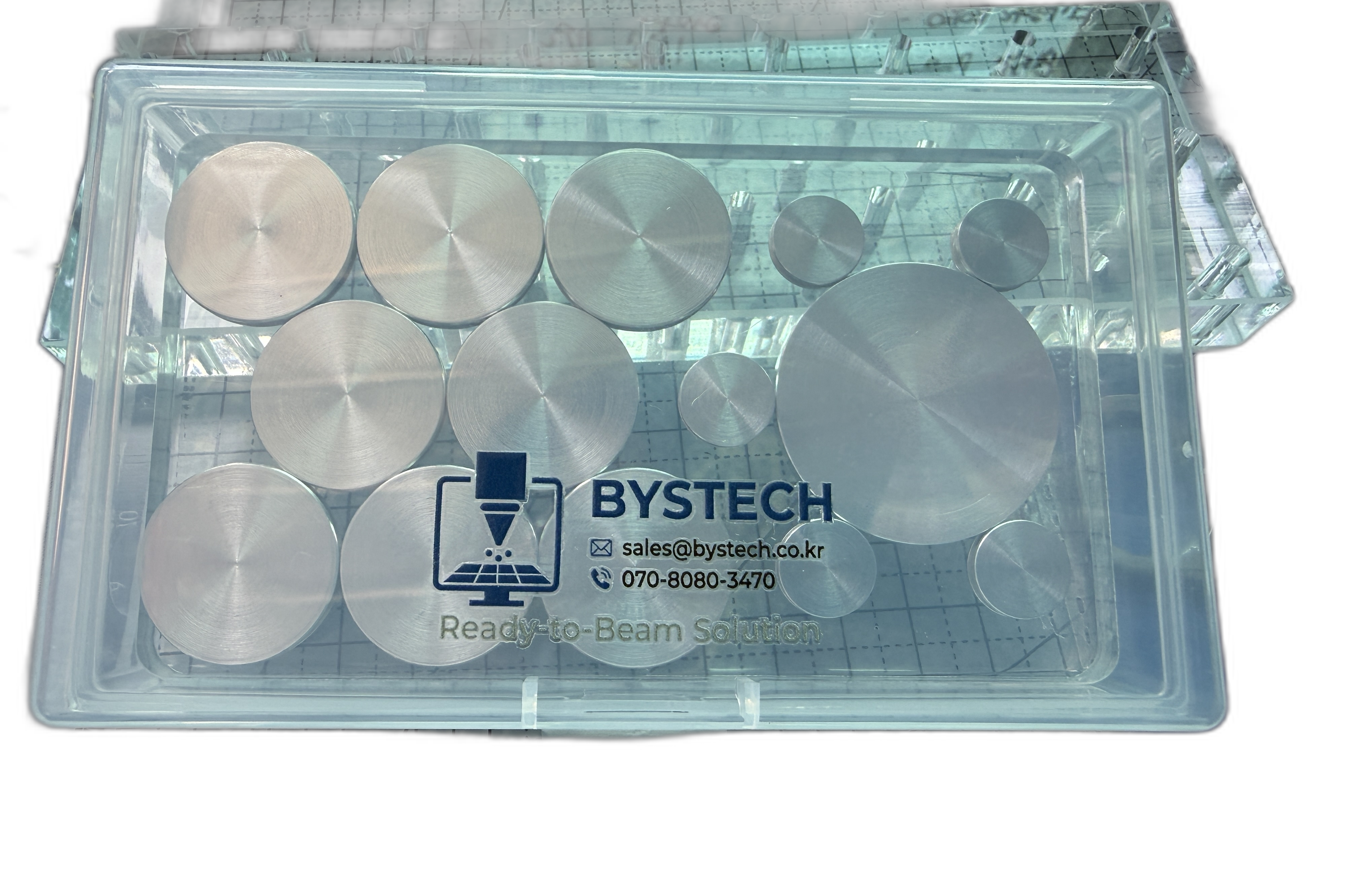
BYSTECH SEM Stub Collection — various aluminum stubs
Instrument Comparison Sample Prep Guide Workflow TEM Guide Grid Material Safety Troubleshooting FAQ

INSTRUMENT COMPARISON

SEM · FIB · TEM Instrument Comparison

Understanding the characteristics and purpose of each instrument clarifies consumable selection.

SEM
Scanning Electron Microscope
FIB
Focused Ion Beam
TEM
Transmission Electron Microscope
Resolution 1 ~ 20 nm 2.5 ~ 20 nm 0.1 ~ 0.2 nm
Atomic-level analysis
Sample Requirements Conductive surface required
Sputter coating or conductive specimen
Fixed to Al Stub
FIB Lift-out process applied
Thin section ≤100 nm
Fixed to 3 mm grid
Key Applications Morphology observation, EDS elemental analysis,
surface defect inspection
Cross-section milling, TEM sample prep,
nano patterning
Crystal structure analysis,
atomic-level imaging, interface analysis
Key Consumables Al Stub, Carbon/Silver Tape,
Conductive Paint, Sputter Target
Al Stub, FIB Lift-out Grid,
Carbon Paint
TEM Grid, Support Film,
FIB Lift-out Grid, Grid Box

HANDLING & PREPARATION

SEM Stub Handling & Conductive Adhesives

Prevent specimen contamination and instrument damage through proper handling.

SEM Stub Handling

Mounting & Handling Precautions

  • Always use powder-free gloves and tweezers to prevent pin/needle contamination. Direct contact with bare hands causes oil contamination.
  • Remove dust from the mounting face (base/pin) before securing in the holder. To prevent thread damage, avoid over-torquing. The set screw should be tightened with light hand pressure only (approx. 0.2–0.3 N·m).
  • When using angled/pre-tilt stubs, always verify clearance from the chamber and pole piece before tilting.
  • Mount specimens with the centre of mass as low as possible to prevent vibration (drift) and tipping during high-magnification imaging.
  • After use, store in a dry environment such as a desiccator (relative humidity ≤30–40%RH) to prevent oxidation and corrosion of aluminium/copper surfaces.

Conductive Adhesive & Paint

Conductive Adhesive & Paint Application

  • Before attaching tape/tab, degrease the specimen bottom surface (e.g. IPA) and ensure it is flat to maximise adhesion. After applying IPA, allow 30 seconds to 1 minute to dry completely before mounting.
  • Apply carbon/silver paint in a "bridging" pattern connecting the specimen top to the stub metal body to establish a conductive path.
  • Note: Silver paint may cause Ag peak interference in EDS analysis. For elemental analysis, prefer carbon-based paint.
  • Load the instrument only after the paint has fully dried/cured (to minimise outgassing). General guideline: 15–30 min at room temperature or 5–10 min in a 60°C oven. Allow more time for thick application.
  • When using copper/aluminium tape as a grounding extension, ensure the edges are firmly pressed down to prevent lifting.

Conductive Coating for Non-conductive Specimens

Conductive Coating & Charging Prevention

Non-conductive specimens such as polymers, ceramics, and biological samples cause charging when exposed to the electron beam, resulting in blurred or distorted images. A conductive coating creates a surface conduction path to prevent this.

  • Au/Au-Pd (gold-palladium) is for general morphology observation. A thickness of 5–20 nm in a sputter coater is standard. Use thinner coatings at higher resolution.
  • Carbon coating is recommended for EDS/WDS elemental analysis as it produces no metallic peak interference. A thickness of 10–30 nm with a carbon coater is standard.
  • If your instrument supports Low-Vacuum or ESEM mode, imaging without coating is an alternative option to avoid charging.
  • Note: An excessively thick coating can obscure fine structures and create crack artefacts. Apply the minimum thickness appropriate for the analysis purpose.

SAMPLE PREPARATION WORKFLOW

5-Step Sample Preparation Workflow

Standard sample preparation process for optimal SEM·FIB analysis results.

1
Cleaning
& Fixation
2
Drying
3
Sample
Mounting
4
Sputter
Coating
5
Storage
1

Cleaning & Fixation

Cleaning & Fixation

Remove contaminants from the specimen surface and stabilise for subsequent steps.

  • Use an ultrasonic cleaner to remove surface particles
  • Solvents: apply IPA, acetone, ethanol sequentially
  • Transfer in a contamination-free environment after cleaning
2

Drying

Drying

Completely remove residual moisture and solvents to minimise outgassing.

  • Complete drying at low temperature using a vacuum oven
  • Dry under vacuum conditions to prevent specimen damage
  • Confirm complete drying before proceeding to the next step
3

Sample Mounting

Sample Mounting

Secure the specimen to the Al Stub and establish a conductive path and observation conditions.

  • Fix with Al Stub + Carbon/Metal Tape
  • Remove residual organic contamination with Plasma Cleaner (Ar/O₂ mixed gas, 10–20 W, 30–60 s — use pure Ar or low power for polymer/organic specimens)
  • Tools: Diamond Pencil, Razor Blade, Gel Pack, Vacuum Tweezer
  • Visually verify mounting condition under a Stereo Microscope
4

Sputter Coating

Sputter Coating

Form a metal thin film on non-conductive specimens to prevent charging.

  • Form a PVD conductive film using a Sputter Coater
  • Target material: choose Pt, Au, Ag etc. according to analysis purpose
  • Carbon (C) coating is recommended for EDS elemental analysis
5

Storage

Storage

Safely protect specimens from contamination and oxidation before and after analysis.

  • Vacuum storage using a vacuum desiccator + vacuum pump
  • Use an acrylic stub storage tray to organise and support stubs
  • Maintain humidity ≤30–40%RH, include desiccant

TEM GRID HANDLING & STORAGE

TEM Grid Handling & Storage

TEM grids are extremely delicate consumables. Proper handling and storage determines specimen quality.

TEM Grid Handling

Handling Precautions & Procedures

  • Never touch the foil/film area of the grid directly. Always grip only the edge (rim) with tweezers.
  • Use precision tweezers with no tip wear (Style 3C/5 etc.), or use ESD vacuum tweezers briefly to prevent specimen damage.
  • Grids are highly sensitive to static electricity. Always work with an earthing mat and wrist strap.
  • Wear a mask, and be careful as strong air blowing (air jet) can damage the grid.

Storage & Transportation

Storage Method & Transportation

  • Store horizontally in a GelPak or dedicated grid storage box to minimise specimen movement and physical shock.
  • Include silica gel desiccant and maintain 20–40%RH to prevent oxidation and corrosion.
  • Always label the storage box (specimen ID, grid type/mesh) and clearly mark the orientation.
  • For external transport, use thorough cushion packaging and avoid rapid temperature changes to prevent condensation on specimen surfaces.

TEM GRID MATERIAL GUIDE

TEM Grid Material Selection Guide

Selecting the appropriate grid material based on analysis purpose and sample characteristics improves data reliability.

Material Recommended Use Key Features Notes
Cu
Copper / General
General purpose analysis Most standard and affordable
~90% of total usage
Susceptible to acid
Cu EDS analysis not possible
Ni
Nickel / Bio-immuno
Biological / immunostaining Excellent chemical resistance
Resistant to chemical treatment
Magnetic
Non-magnetic tweezers required
Au
Gold / cell culture
Cell culture / high corrosion resistance Best biocompatibility
No oxidation or corrosion
Essential for Immunogold Labeling
Most expensive
Somewhat lower mechanical strength
Mo
Molybdenum / FIB+high-temp
FIB / high-temperature experiments High melting point, low thermal expansion
High hardness, resistant to FIB ion beam
Somewhat demanding to handle
For special purposes, check stock availability
Nylon
Cryo-TEM
Cryo-TEM / lightweight analysis Non-magnetic, biocompatible
Usable at cryogenic temperatures
Heat sensitive
Not suitable for high temperatures
SiN
Liquid TEM
Liquid TEM / in-situ experiments Ultra-thin window structure
Real-time observation possible
Very fragile
Special handling required

3-Step Checklist for Selecting the Right Grid Material

1

Are you performing EDS (elemental analysis)?

YES → Choose a grid material different from the elements present in your specimen.
Example: copper alloy specimen → recommend Ni or Mo grid

2

Performing complex chemical treatment or staining?

YES → Choose Ni (nickel) or Au (gold), which are resistant to acids and solvents.
Cu may react with reagents and produce noise.

3

FIB milling or high-temperature heating experiment?

YES → Mo (molybdenum), with no thermal deformation and high rigidity, is essential.

TROUBLESHOOTING

Troubleshooting Guide

Common symptoms, causes, and solutions encountered in the field.

SYMPTOM

Image brightens/washes out or shakes (Charging)

CAUSE

No conductive path, missing coating or broken paint bridge

SOLUTION

Re-apply carbon paint bridging between specimen and stub, check conductive coating thickness, reduce accelerating voltage (e.g. 1–5 kV)

SYMPTOM

Image drifts to one side at high magnification (Drift)

CAUSE

Unstable specimen fixation, paint/tape outgassing, thermal non-equilibrium

SOLUTION

Secure firmly with lower centre of mass, load instrument only after paint fully cures, wait a few minutes to stabilise before imaging

SYMPTOM

Unexpected peaks detected in EDS spectrum

CAUSE

Ag peak from silver paint, Au/Pd coating peak, tape adhesive components

SOLUTION

Switch to carbon-based paint/coating for elemental analysis, exclude coating elements from analysis targets

SYMPTOM

TEM grid support film is torn or wrinkled

CAUSE

Excessive tweezer grip pressure, strong air blowing, incorrect pickup direction

SOLUTION

Grip only the edge with Style 5 precision tweezers, avoid air blowing, consistently handle with film side facing up

SYMPTOM

Specimen/stub surface discolouration or corrosion

CAUSE

Storage in high-humidity environment, salt/oil residue from bare-hand contact

SOLUTION

Store in desiccator (≤30–40%RH), include desiccant, always use gloves and tweezers

SAFETY PRECAUTIONS

Safety Precautions

Safety requirements that must be observed when handling analytical instrument consumables.

Volatile Solvents / Outgassing

Volatile Solvents & Outgassing

  • Work in a well-ventilated area or under a local exhaust ventilation system (Fume Hood).
  • When handling flammable materials, observe no open flames and remove all heat sources.
  • Wear appropriate PPE including safety goggles, nitrile gloves, and organic solvent mask.

Sharp Tools / Blades

Sharp Tools & Blades

  • Take great care of laceration risk when using razor blades, precision tweezers, etc.
  • Always work on a cutting mat and keep fingers away from the direction of the blade.
  • Dispose of used sharp consumables in designated sharps disposal containers.

Static Electricity / High Voltage

Static Electricity & High Voltage

  • Use ESD grounding strap and mat to protect sensitive electronic components.
  • Before work, verify the instrument grounding status to prevent leakage current.
  • Before maintenance or cleaning, cut the main power supply and discharge residual charge.

FIB Ion Beam Safety (Ga)

FIB Ion Beam Safety

  • Nitrile gloves and safety goggles are mandatory when handling gallium (Ga) ion source.
  • Use a dedicated absorption kit when removing gallium residue from the chamber and maintain adequate ventilation.
  • The ion beam cannot be seen with the naked eye, so opening the chamber during instrument operation is strictly prohibited.

FAQ

Frequently Asked Questions

The most commonly asked questions from our customers.
What is the difference between carbon paint and silver paint?
Silver (Ag) paint offers excellent conductivity and adhesion, making it suitable for general morphology observation. However, it can cause interference in EDS elemental analysis due to detected Ag peaks. Carbon paint has slightly lower conductivity but produces less interference during analysis. For quantitative or qualitative elemental analysis, carbon-based paint is recommended.
Can SEM stubs be reused?
Aluminium stubs can be reused after cleaning residual paint, tape, and specimen material with a solvent (e.g. IPA) and light polishing if needed. However, reuse is not recommended for trace analysis where cross-contamination is critical, or for stubs with damaged or oxidised surfaces.
Are TEM grids single-use?
Grids with a support film (Formvar, carbon) should effectively be treated as single-use. The film is easily damaged during specimen removal, and there is a risk of cross-contamination. Bare mesh grids can sometimes be cleaned and reused, but for analytical reliability, using new grids is recommended.
Is coating mandatory for non-conductive samples?
In high-vacuum SEM, conductive coating is recommended for non-conductive specimens such as polymers, ceramics, and biological samples to prevent charging. However, instruments that support Low-Vacuum or Environmental SEM (ESEM) mode allow imaging without coating. This approach is advantageous when preserving the original specimen form is important.
How do I confirm stub compatibility with my instrument?
Stub diameter (e.g. Ø12.7mm, Ø25.4mm) and pin specification (e.g. Ø3.2mm) vary by SEM manufacturer and model. Please provide your instrument model name and we will confirm the compatible specifications. Non-standard holders can also be custom fabricated.

Purchase Consumables or Further Enquiries

If you need the consumables mentioned in this guide, contact us via inquiry form or request a quote.

Naver Store Get a Quote